Course Overview
IPC A610J Acceptability of Electronic Assemblies Training
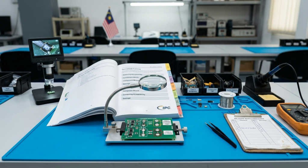
These 2 days training and qualifying workshop in IPC A610J will provide the participants with knowledge and skills required in understanding all aspects of IPC A610J standards including product classifications, components and solderability accept/reject criteria, defects categories in detailed technical perspective plus product solder defects identification to enhance the learning.
This IPC A610J Training provides comprehensive understanding of electronic assembly acceptability requirements, inspection criteria, soldering standards, and quality control practices based on the latest IPC A610J specifications. Participants will gain practical knowledge to identify defects, evaluate product quality, and improve electronic assembly processes.
Course Objectives
Enhance knowledge and skills in the following areas:
Know IPC A610J new inclusions.
Understand the terminologies, terms and definitions.
Able to know IPC610 standards and its requirements to build quality products.
Know the 3 types of Product Classifications.
Know how to apply Inspection methodology – Form, Fit and Function.
Accept and Reject criteria of electronic components and solderability in interconnects, packaging and electronic circuits.
Documents applicable to IPC A610J.
Expose to close and open book tests, assessment and qualification.
Establish certification through qualifying Pre and Post Tests.
Get qualified and Competent in IPC A610J with great negotiating skills with customer on return goods criteria.
Able to train operators in process standards to maintain product quality.
Through this IPC A610J Training, participants will develop the ability to interpret industry standards, perform effective inspection methods, and apply acceptance criteria for electronic assemblies. The programme supports engineers, technicians, and quality personnel in maintaining consistent product quality and meeting customer requirements.
Who Should Attend
Engineers, Technicians, Line Trainers and Production / QA Inspectors.
This IPC A610J Training is suitable for professionals involved in electronic manufacturing, quality assurance, inspection, production processes, and assembly improvement activities.
Workshop Methodology
Participants will be involved in 60% lectures and 40% group and team discussions. Grading for certification is achieved by tests via open and close book exams.
Course Details
Duration
2 Days (9:00 am to 5:00 pm)
Course Content
Day 1: Lesson Plan
Pre-Test: Objective – 20 questionnaires assessment.
Exercise 1: List down all defects encountered in products and processes that affect quality.
Introduction to IPC A610J (What, Why, Who, When, How).
IPC-A-610J – March 2024 – Standards Acceptability of Electronic Assemblies
1.0 General (Scope, Purpose, Classification, Measurement Units and Applications, Verification of Dimensions, Requirements)
1.5.1 Acceptance Criteria (Acceptable, Defect, Disposition, Process Indicator, Conditions Not Specified, Specialized Designs, Shall / Should)
1.6 Process Control Methodologies & 1.7 Order of Precedence (Clause References, Appendices)
1.8 Terms and Definitions (Board Orientation, Primary Side, Secondary Side, Solder Source Side, Solder Destination Side, Bridging Bubble, Cold Solder Connection, Common Conductors, Conductor Overlap, Conductor Overwrap, Diameter, Electrical Clearance, Engineering Documentation, FOD – Foreign Object Debris, Form, Fit, Function – F/F/F, High Voltage, Intrusive Solder, Kink, Locking Mechanism, Manufacturer, Meniscus – Component, Noncommon Conductors, Nonfunctional Land, Pin-in-Paste, Solder Balls, Standard Industry Practice – SIP, Stress Relief, Supplier, Tempered Leads, User)
1.10 Personnel Proficiency & 1.11 Acceptance Requirements (Missing Parts and Components, Jumper Wire)
1.12 Minimum Electrical Clearance (MEC) & 1.13 Inspection Methodology (Lighting, Magnification Aids)
2.0 Applicable Documents (IPC Documents, Joint Industry Documents, Electrostatic Association Documents, International Electrotechnical Commission Documents, ASTM, Military Standards, SAE International)
3.0 Handling Electronic Assemblies
4.0 Hardware
Hardware Installation (Electrical Clearance, Interference, Component Mounting – High Power, Heatsinks, Insulators and Thermal Compounds, Contact)
Threaded Fasteners and Other Threaded Hardware (Torque, Solid Wires, Stranded Wires)
Jackpost Mounting & Connector Pins (Edge Connector Pins, Press Fit Pins, Land/Annular Ring, Soldering)
Wire Bundle Securing & Routing (Wires and Wire Bundles)
5.0 Soldering
Soldering Acceptability Requirements
Soldering Anomalies (Exposed Basis Metal, Pin Holes/Blow Holes/Voids, Reflow of Solder Paste, Nonwetting, Cold Connection, Dewetting)
Excess Solder (Solder Balls, Bridging, Solder Webbing/Splashes)
Disturbed Solder, Cooling Lines and Secondary Reflow, Fractured Solder, Solder Projections, Pb-Free Fillet Lift, Pb-Free Hot Tear/Shrink Hole, Probe Marks and Other Similar Surface Conditions in Solder Joints, Inclusions
Partially Visible or Hidden Solder Connections, Heat Shrinkable Soldering Devices
6.0 Terminal Connections
Swaged Hardware (Terminals, Terminal Base to Land Separation, Turret, Bifurcated, Rolled Flange, Flared Flange, Controlled Split, Solder)
Insulation (Damage, Presolder, Post-Solder, Clearance, Insulation Sleeving, Placement, Damage)
Conductor (Deformation, Damage, Stranded Wire, Solid Wire, Strand Separation/Birdcaging – Presolder & Post-Solder, Tinning)
Service Loops, Routing (Wires and Wire Bundles – Bend Radius), Stress Relief (Wire)
Lead/Conductor Placement & Solder General Requirements
Turrets and Straight Pins (Conductor Placement, Solder)
Bifurcated (Conductor Placement, Side Route Attachments, Staked Wires, Bottom and Top Route Attachments, Solder)
Slotted, Pierced/Perforated, Hook, Solder Cups (Conductor Placement, Solder)
AWG 30 and Smaller Diameter Wires, Series Connected, Edge Clip Position
Day 2: Lesson Plan
7.0 Through-Hole Technology
Component Mounting (Orientation – Horizontal/Vertical, Lead Forming, Bend Radius, Space between Seal/Weld and Bend, Stress Relief, Damage, Leads Crossing Conductors, Hole Obstruction, DIP/SIP Devices and Sockets, Radial Leads – Vertical/Horizontal, Spacers, Connectors, Right Angle, Vertical Shrouded Pin Headers and Vertical Receptacle Connectors)
Component Securing (Mounting Clips, Adhesive Bonding, Nonelevated Components, Elevated Components, Other Devices)
Supported Holes (Axial Loaded – Horizontal/Vertical, Leads/Conductors Protrusion, Lead/Conductor Clinches)
Supported Holes Solder (Vertical Fill – A, Solder Destination Side – Lead to Barrel – B, Solder Destination Side – Land Area Coverage – C, Solder Source Side – Lead to Barrel – D, Solder Source Side – Land Area Coverage – E)
Solder Conditions (Solder in Lead Bend, Touching Through-Hole Component Body, Meniscus in Solder, Lead Cutting After Soldering, Coated Wire Insulation in Solder, Interfacial Connection without Lead – Vias, Board in Board)
Unsupported Holes (Axial Leads – Horizontal/Vertical, Wire/Lead Protrusion, Wire/Lead Clinches, Solder, Lead Cutting After Soldering)
8.0 Surface Mount Assemblies
Staking Adhesive (Component Bonding, Mechanical Strength)
SMT Leads (Plastic Components, Damage, Flattening)
SMT Connections & Chip Components (Bottom Only Terminations, Side Overhang – A, End Overhang – B, End Joint Width – C, Side Joint Length – D, Maximum Fillet Height – E, Minimum Fillet Height – F, Solder Thickness – G, End Overlap – J)
Rectangular or Square End Chip Components – 1, 2, 3 or 5 Side Termination(s) (Side Overhang – A, End Overhang – B, End Joint Width – C, Side Joint Length – D, Maximum Fillet Height – E, Minimum Fillet Height – F, Solder Thickness – G, End Overlap – J)
Termination Variations (Mounting on Side/Billboarding, Mounting Upside Down, Stacking, Tombstoning)
Center and Lateral Terminations (Solder Width of Side Termination, Minimum Fillet Height of Side Termination)
Cylindrical End Cap Terminations (Side Overhang – A, End Overhang – B, End Joint Width – C, Side Joint Length – D, Maximum Fillet Height – E, Minimum Fillet Height – F, Solder Thickness – G, End Overlap – J, Center and Lateral Terminations)
Castellated Terminations (Side Overhang – A, End Overhang – B, Minimum End Joint Width – C, Minimum Side Joint Length – D, Maximum Fillet Height – E, Minimum Fillet Height – F, Solder Thickness – G)
Flat Gull Wing Leads (Side Overhang – A, Toe Overhang – B, Minimum End Joint Width – C, Minimum Side Joint Length – D, Maximum Heel Fillet Height – E, Minimum Heel Fillet Height – F, Solder Thickness – G, Coplanarity)
Round or Flattened/Coined Gull Wing Leads (Side Overhang – A, Toe Overhang – B, Minimum End Joint Width – C, Minimum Side Joint Length, Maximum Heel Fillet Height, Minimum Heel Fillet Height, Solder Thickness – G, Minimum Side Joint Height – Q, Coplanarity)
J Leads (Side Overhang – A, Toe Overhang – B, End Joint Width – C, Side Joint Length – D, Maximum Heel Fillet Height – E, Minimum Heel Fillet Height – F, Solder Thickness – G, Coplanarity)
Butt/I Connections (Modified Through-Hole Terminations, Maximum Side Overhang – A, Toe Overhang – B, Minimum End Joint Width – C, Minimum Side Joint Length – D, Maximum Fillet Height – E, Minimum Fillet Height – F, Solder Thickness – G)
Solder Charged Terminations (Maximum Side Overhang – A, Maximum Toe Overhang – B, Minimum End Joint Width – C, Minimum Fillet Height – F)
Flat Lug Leads, Tall Profile Components Having Bottom Only Terminations, Inward Formed L-Shaped Ribbon Leads
Surface Mount Area Array (Alignment, Solder Ball Spacing, Solder Connections, Vias/Voids, Underfill/Staking, Package on Package)
Bottom Termination Components (BTC), Components with Bottom Thermal Pad Terminations (D-Pak)
Flattened Post Connections (Maximum Termination Overhang – Square/Round Solder Land, Maximum Fillet Height)
P-Style Terminations (Maximum Side Overhang – A, Maximum Toe Overhang – B, Minimum End Joint Width – C, Minimum Side Joint Length – D, Minimum Fillet Height – F)
Vertical Cylindrical Cans with Outward L-Shaped Lead Terminations, Flexible and Rigid Flex Printed Circuitry with Flat Uniformed Leads
Wrapped Terminals (Side Overhang – A, End Joint Width – C, Side Joint Length – D, Minimum Heel Fillet Height – F, Solder Thickness – G), Flat Leaded Surface Mount Connectors
Specialized SMT Terminations & Surface Mount Connectors (Surface Mount Threaded Standoffs – SMTS / Surface Mount Fasteners)
9.0 Component Damage
Loss of Metallization, Chip Resistor Element, Leaded/Leadless Devices, Ceramic Chip Capacitors, Connectors, Relays, Ferrite Core Components, Connectors/Handles/Extractors/Latches, Edge Connector Pins, Press Fit Pins, Backplane Connector Pins, Heatsink Hardware, Threaded Items and Hardware
10.0 Printed Boards and Assemblies
Non-Soldered Contact Areas (Contamination, Damage)
Laminate Conditions (Measling and Crazing, Blistering and Delamination, Weave Texture/Weave Exposure, Haloing, Nicks and Cracks, Burns, Bow and Twist, Depanelization, Mechanical Damage)
Conductors/Lands (Reduction, Lifted, Mechanical Damage)
Flexible and Rigid-Flex Printed Boards (Damage, Delamination/Blister – Flex & Flex to Stiffener, Solder Wicking, Attachment)
Marking (Etched/Hand Printing, Screened, Stamped, Laser, Labels, Bar Coding/Data Matrix, Readability, Adhesion and Damage, Position, RFID Tags)
Cleanliness (Flux Residues, Cleaning Required, No Clean Process, Foreign Object Debris – FOD, Chlorides, Carbonates and White Residues, Surface Appearance)
Solder Mask Coating (Wrinkling/Cracking, Voids, Blisters, Scratches, Breakdown, Discoloration)
Conformal Coating & Electrical Insulation Coating (General, Coverage, Thickness), Encapsulation
11.0 Discrete Wiring (Solderless Wrap)
12.0 High Voltage
13.0 Jumper Wires (Wire Routing, Wire Staking – Adhesive or Tape, Terminations, Lap – Component Lead/Land, Wire in Hole, Wrapped, SMT – Chip and Cylindrical End Cap Components/Gull Wing/Castellations)
Appendix A: Protecting the Assembly — ESD and Other Handling Considerations
ESD Prevention (ESD Control Program, ESD Protective Area – EPA Requirements, Minimizing Static Charge, ESD Protective Packaging, Training, Tools And Equipment, Compliance Verification, Warning Labels)
General Handling (Handling Considerations, Preventing Contamination, Gloves and Finger Cots)
Moisture Sensitive Devices
Conclusion & Assessment
Summary – Day 1 and 2 lessons recap
Post-Test Assessment
Pre and Post-Tests – Exam review and scoring
Training Evaluation